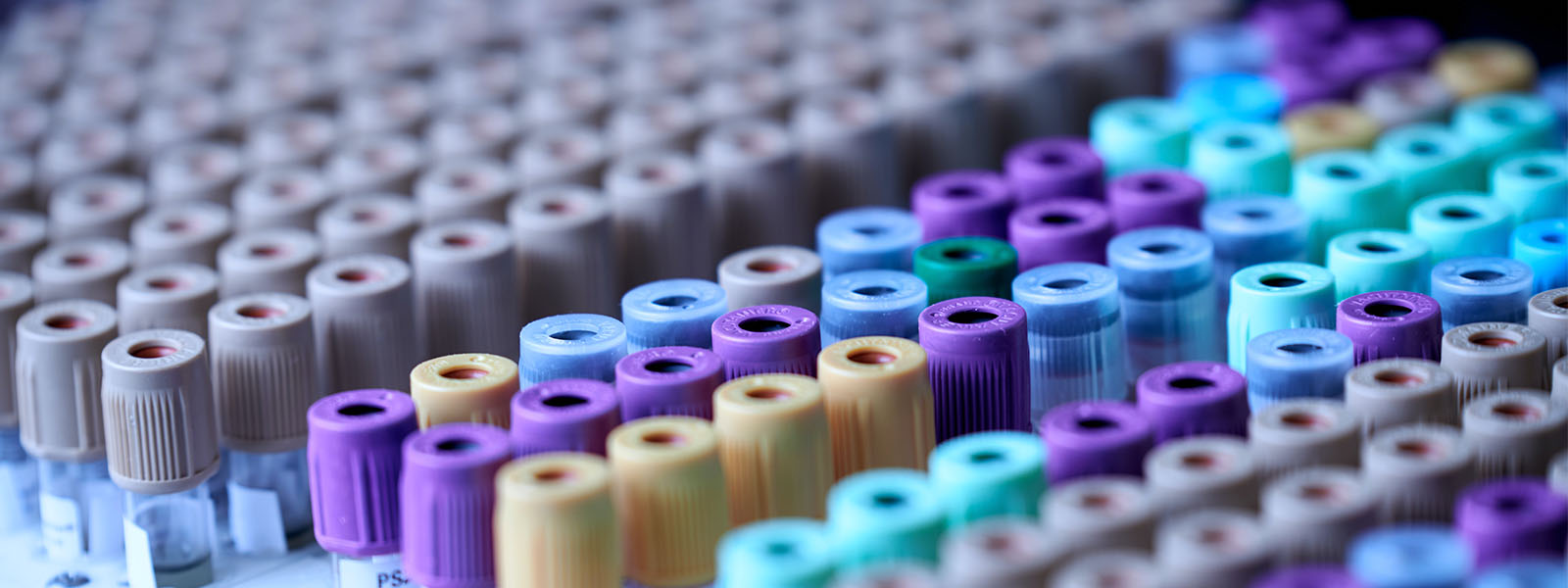
Scanning Electron Microscopy
Scanning electron microscopy produces sharp, high-resolution, black-and-white images of samples. The outputs give researchers topographical, morphological and compositional information to support medical, biological, material sciences and engineering.
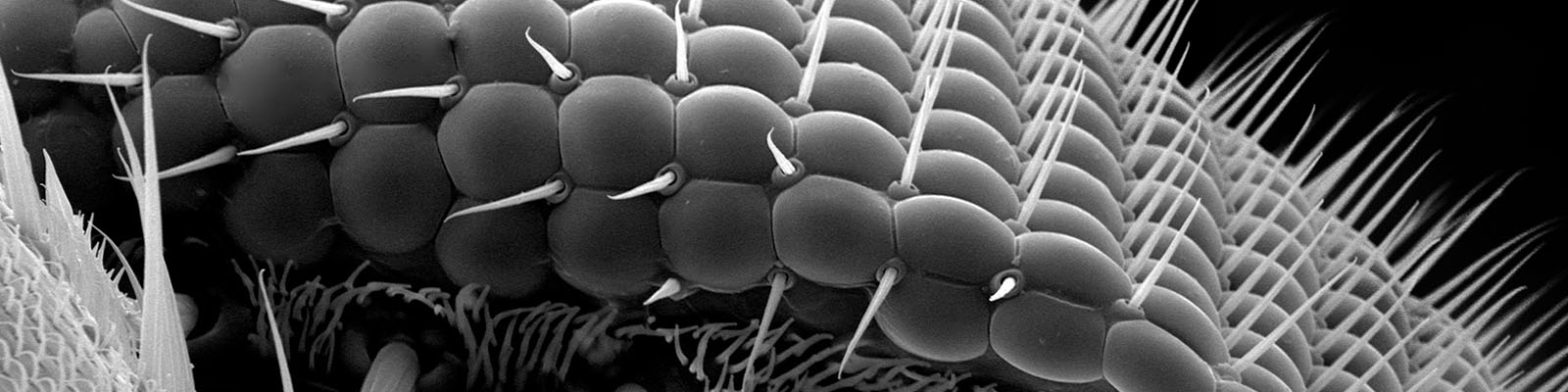
Provides a broad range of surface imaging capabilities and elemental analysis for both conductive and non-conducting samples.
Supports medical, biological and material sciences.
Technical specifications
- Field-emission electron source and advanced optics enable high resolution field-free imaging at low accelerating voltage with in-lens secondary electron (SE) detector
- SE detector is used in field-free mode for comprehensive low to high magnification imaging of a variety of samples
- Back scattered electron detector with a Bruker SDD EDS detector supports visualisation of compositional differences across the specimen surface
- Bruker SDD EDS detector enables analysis of elements down to Boron (atomic number 5)
- Variable-pressure (low vacuum) mode supports imaging of non-conductive and vacuum-sensitive specimens
Coming in December 2022
- With a suite of state of-the-art technologies, this instrument is a multi-functional workstation designed to carry out ultra-high-resolution imaging (2D and 3D), microanalysis (2D and 3D), high quality TEM specimen preparation, nanoscale and micro-scale milling, deposition, and fabrication
Ideal for use in medical, biological, and material sciences.
Technical specifications
- Ultra-high-resolution imaging below 1nm resolution in both 2D and 3D imaging
- Wide array of detectors and advanced optics allowing high-contrast, field-free imaging at low accelerating voltages
- A new generation of 2.5µA Xe plasma FIB ion column provides unique and fast ion milling capabilities (with 50x higher throughput compared to that in a Ga-based FIB)
- Rapid cross-sectioning of technical specifications up to 900 µm.
- Extended 3D analytical capabilities including EDS with FEI UltraDry 100M SDD EDS system
- Equipped with an easy-lift micromanipulator for in-situ TEM and atom probe sample lift-out
The University of Newcastle acknowledges the traditional custodians of the lands within our footprint areas: Awabakal, Darkinjung, Biripai, Worimi, Wonnarua, and Eora Nations. We also pay respect to the wisdom of our Elders past and present.